| Overview |
| |
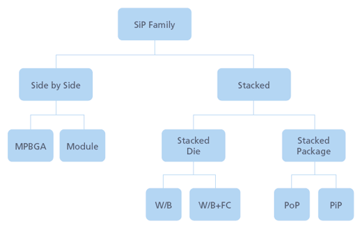
| System-in-Package (SiP) meets growing demands for semiconductor miniaturization and multiple functions. SiP performs full functional system or sub-system functions at the package level. SiP has evolved into 2D & 3D integrated modules of several chip packages lined up side by side or stacked, or adding passives or other required components into the package to build a full sub-system function. SiP main applications are 4C products including Computer, Communication, Consumer and Car electrics. Industry and market trend shows great convergence of 4C’s in hand held products such as Cell Phone, GPS, PDA and so on. SiP main strategy are Small form factor, Innovated function, Flexible design, System integrated, High electrical performance, Low cost and Time to market. Two major SiP package family groups offered at ASE including die combination and package combination. Wire bonding, Flip Chip and SMT are major interconnection technologies. |

|
| Application |
| |
| MPBGA is KGD solution and integrates multi functional components in package level to provide high speed and high performance sub-system solution. It consists of Wire bonding, Flip Chip, utilizes advanced substrate technology and surface mount technology to enable flexibility in design and efficiency in production. |
|
| Module |
| |
| A fully functional sub-system in a fine geometry package format in LGA or BGA. One or more active IC with multiple chip-level interconnections (W/B or Flip Chip) and consist of a substrate (Laminate or Leadframe or Ceramic or Silicon). |
|
| Stacked die |
| |
| Stacked die package is typical and major running type of SiP product. Stacked die package adopts vertical stacking between die to die for combining several devices into single package form factor. It can significantly improve electrical performance by sorting the signal communication path between the devices and reducing system level size by performing subsystem function from the PCB board to the package. The stacked methodology included Wire Bond, Spacer, Die overhang and Flip Chip technology to achieve flexible design & structure. |
|
| Staked Package |
| |
| Stacked Package is KGD package solution including PiP (package in package) and PoP (package on package). The Stacked package adopts 3D idea. Each package is individually assembled and tested before integrated. This is also solution to improve package burn in test yield performance. |
| |
 |
|