 |
|
|
| Bumping |
 |
| Product Overview |
| |
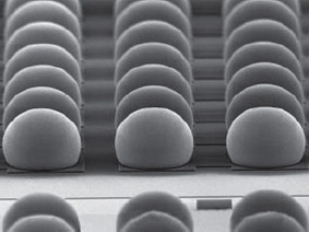
Wafer bumping is an essential to flipchip or board level semiconductor packaging. Bumping is an advanced wafer level process technology where “bumps” or “balls” made of solder are formed on the wafers in a whole wafer form before the wafer is being diced into individual chips. Those “bumps”, which can be composed from eutectic, lead free, high lead materials, or Cu pillar on wafer are the fundamental interconnect components that will interconnect the die and the substrate together into a single package. These bumps not only provide a connected path between die and substrate, but also play an important role in the electrical, mechanical and thermal performance in the flipchip package.
Flip chip assembly package has traditionally been used for high-end niche applications. Recent technology development has adopted this process to be widely used in today’s consumer electronics applications. For the performance driven market, flip chip interconnection reduces signal propagation delay, provide much better bandwidth, and relieves the constraints of power and ground distribution. For the form factor driven market, such as mobile applications, replacing wire bonding by flip chip interconnects reduces the size and weight of the package.
As the world leading IC assembly subcontractor, ASE established its wafer bumping services in 1999. Licensed from Flip Chip International, LLC, the world’s leader in printing bumping technologies, ASE’s flip chip bumping process has proven to be robust and reliable, with production experience accumulated since 2000 as the very first subcontractor to provide large volume production in bumping service.
ASE also established the plating bump process in 2003. The plating process has proven the robustness, reliability, and provided production service. |

|
| ASE's Wafer Bumping Capabilities |
| |
Currently, ASE operates three state-of-the-art bumping facilities with varieties of bumping processes available, two are for 150mm and 200mm wafer, one is for 300mm wafer, all located in Kaohsiung, Taiwan. During the first quarter of 2000, ASE’s 200mm printing bumping process successfully passed the internal package reliability test. The bumping process was later qualified by customers and began volume production in the third quarter of 2000. The 300mm printing line was established in 2002 and turned into production since third quarter of 2002. To date, more than 1 million 6” & 8” wafers from over 100 customers’ device, more than 0.3 million 12” wafers from over 16 customer’s device have been processed in ASE’s printing bumping facilities with consistent output of over 70k 6”& 8” wafers per month, over 11k 12” wafers per month. More than 0.1 million 12” wafers from over 10 customer’s device have been processed in ASE’s plating bumping facilities with consistent output of over 6k wafers per month.
As a leader of bumping process provider, ASE began to develop and construct not only solder bump process, but also Cu pillar process. Cu pillar structure is applied for fine pitch, lead-free, or high current application device. |
|
| Features |
| |
| High density interconnection |
| High-speed data processing |
| Fine bump pitch (array and peripheral) |
|
|
| Advanced Bumping Technologies under Development |
| |
| ASE continues to invest in advanced technologies to maximize solutions for customers’ sophisticated chip designs. We are currently working with major IDMs and the world’s top foundries on polyimide Repassivation and RDL, Cu pillar and 65nm, 45nm cu low-K wafer bumping. Combined with other ASE manufacturing services including substrate design, substrate manufacturing, wafer sorting, bumping, backside grinding, backside marking, flip chip assembly, final test, and drop ship, ASE offers customers unsurpassed flip chip turnkey solutions. |
|
|
|