 |
|
|
| SiP SiP Module |
 |
| Product Overview |
| |
The system-in-Package (SiP) module market has grown signifi cantly over the past several years and it is now one of the fastest growing packaging technologies in the semiconductor industry driven by lower cost, smaller form factor, higher levels of integration and better performance. SiP modules are highly adopted by end customers for wireless communication applications including the RF sections of mobile phone and wireless connectivity. ASE Group, who is already the leader in SiP module manufacturing in terms of experience, technology and capacity, is committed to provide extra value to customers by providing turnkey SiP module total solution.
What is System-in-Package (SiP) Module?
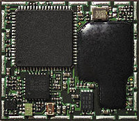
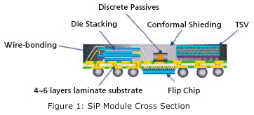
A SiP Module is a fully functional subsystem, which uses a carrier to combine one or multiple IC chips and passive components in a BGA/LGA package form factor. The IC chips (from heterogeneous technologies such as CMOS, BiCMOS, GaAs and others) are either flip-chipped or wire-bonded onto the carrier like leadframe, laminate or LTCC substrate. Passive components such as resistor, capacitor, inductor and filters (SAW/BAW/Balun) are incorporated into the module in the form of discrete passives, integrated passive devices or embedded passives in the substrate. Quite often, a protective casing like metal lids or over-mold encapsulation is included in order to provide mechanical protection and implement EMI shielding at module level. |

|
| Application |
| |
| SiP technology attempts to combine all of the components of a particular function onto a single device through advanced packaging instead of monolithically through silicon integration. The ability to integrate different die technologies and to reduce total product cost and time-to-market are the prime drivers for SiP technology. With these key attributes, SiP module is widely used in wireless or RF applications such as |
1. Power Amplifiers
2. Transceiver
3. Front-end module
4. Antenna switch module
5. Bluetooth
6. WLAN (802.11 a/b/g)
7. GPS/AGPS
8. Mobile-TV (DVB-T/H, DMB, ISBD-T)
9. WiMax (802.16e) |
|
| Key Benefits of ASE’s SiP Modules |
| |
Shorter time-to-market: System level design time is significantly reduced as individual components of the SiP are concurrently developed, ultimately meaning that products can be brought to market faster. SiP is a high value-add product for end users.
System design integration: SiP modules reduce the complexity of the PCB by moving the routing complexity to the module substrate. As a result, the PCB layer count is simplified and reduces the burden for system designers. An SiP module can serve as a plug and play functional block and enable system designers to add additional functions onto the system using minimal design effort.
Simplified system test: All shipped SiP modules are pre-tested and pre-qualified. Thus, it simplifies system testing equipment requirement and reduces production test time at OEM manufacturing level.
Easy logistic management: SiP modules reduce the number of items in inventory and help to reduce the manufacturing steps required at board level.
Higher production efficiency and yield: Stringent test procedures are carried out throughout the SiP module development level, where each component is thoroughly tested individually. This results in a higher yield once the SiP is tested at board level. |
|
| ASE SiP Module Capabilities |
| |
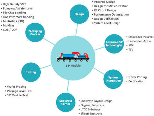 |
|
| Service Offering |
| |
SiP is the ideal solution for system integration. ASE is committed to work with customers to devise optimized SiP module solutions, offering strong advantages in cost, size and performance, less design interaction, and shorter development cycle. Our SiP module engineers understand customer concerns and are experienced in identifying multiple options for engineering tradeoffs.
The ASE SiP module engineering team offers the following service to customers:
System Integration
• GSM/CDMA/WCDMA
• Bluetooth/WLAN (802.11 a/b/g)
• GPS
• Mobile TV: DVB-T/DVB-H
• WiMax
SiP Module Co-Design
• Reference design and schematic translation
• RF Circuit design
- RF characterization
- R/L/C components
- RF filters: BALUNS, LPF, HPF, BPF, SAW/BAW
- Matching circuitry
- Simulation Tools: Agilent ADS, Momentum, HFSS
• Antenna Design
• Shielding Solution
• Substrate Layout design
- Laminate substrate
- LTCC substrate
- Layout Tools: Cadence APD, Autocad, Synopsys
Packaging Consultancy
• Package selection & configuration
• Design rule guideline
• Process capability
SiP Module Test Consultancy
• RF Wafer probing
• RF ATE Platform
• EVB design & fabrication
• Testing tooling design & manufacturing
• Final test solution development
- Equipment selection & configuration
- Test software development
- Automated pick & place |
|
| ASE Qualified Processes for Wireless SiP Module |
| |
1. High density and fine pitch SMT
2. EMI shield-lid housing
3. Fine pitch wire bonding
4. Multi-stacked-die packaging
5. Flip chip
6. Wafer level packaging
7. Multi-chip packaging
8. Vacuum assisted mold application
9. Built in passives
10. Pb - & Hologen - free packaging |
|
|
|