| Product Overview |
| |
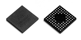
| Land grid array (LGA) uses laminate substrate to form the landing pad and the exposed pad for performance enhancement. It is essentially a BGA minus the solder balls. LGA’s advantage over other leadless packages are its flexible routing and multi-chip module capability. LGA is also a thinner (down to 0.5 mm) and lighter CSP. LGA technology has been developed for lead free solution and spacing reduction on mother boards. This type of package has chip size solution based on mature laminated substrate technology and material. |

|
| Application |
| |
| LGA is suitable for high performance ICs like Single Chip, CPU, Logic and Memory. Common applications for this type of package includes: |
Telecommunication
products
Cellular phone-RF Devices
Wireless LAN
Portable products
Personal digital assistants
Digital camera
IC recorders
MP3 players
Memory
card
SD card
MS card
PCMCIA
Compact |
|
| Features |
| |
| Thinner, lighter and smaller Chip-Scale Package |
Mature standard matrix BGA assembly process
 Higher yield/quality Higher yield/quality
Higher though-put
Lower cost |
| Space reduction in system level |
| Pb free solution |
| Excellent electrical and thermal performance |
|
|
| Reliability |
| |
| Test Item |
Reference Standard |
Condition/Duration |
| MSL |
JEDEC22-A103 |
Level 3, 30°C/60% RH, 192 hrs |
| TCT |
JEDEC 22-A104-B |
-65°C to 150°C, 1000 cycles |
| HAST |
JEDEC 22-A118 |
130°C/85% RH, 33.5 psi 96 hrs |
| HTST |
JEDEC 22-A103-B |
150°C, 1000 hrs |
|
|