| Product Overview |
| |
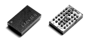
A chip size package (CSP) has a packaged size of no larger than 120 percent of the naked die. In 2001, ASE licensed the Ultra CSP?from Kulicke & Soffa's Flip Chip Division. The Ultra CSP is a wafer level CSP and it does not use an interposer that contributes to a higher cost solution than standard surface mount packages. Another advantage of the Ultra CSPis that it enables direct contact between the device and product because the process uses solder balls instead of wire bonding for interconnection. Signal inductance is significantly redcuced since the interconnects are much shorter than wire bonding. is a wafer level CSP and it does not use an interposer that contributes to a higher cost solution than standard surface mount packages. Another advantage of the Ultra CSPis that it enables direct contact between the device and product because the process uses solder balls instead of wire bonding for interconnection. Signal inductance is significantly redcuced since the interconnects are much shorter than wire bonding. |

|
| Application |
| |
| Applications of Ultra CSP include analog devices, microcontrollers, integrated passives and memories such as Flash, DRAM, SRAM and EEPROM. |
|
| Features |
| |
 Real chip size (smallest, thinnest and lightest) Real chip size (smallest, thinnest and lightest)
High density interconnection
High-speed data processing
Batch process-assembly, processed in wafer form
Wire-bond die type can be directly switched to Ultra CSP® |
|
| Reliability |
| |
| Package Level |
| TCT |
JEDEC 22, A104-A condition B, -55°C~125°C |
1000 cycles |
| PCT |
JEDEC 22B, A102-B, 121°C/15 psig/100% RH |
96 hours |
| THT |
JEDEC 22B, A101-A, 85°C/85% RH |
168/500/1000 hours |
| HTST |
JEDEC 22B, A103-A, 150 |
1000 hours |
|
| |
| Board Level |
| TCT |
-40°C~125°C |
500 cycles |
| Bending test |
1 mm@1Hz |
63.2% failure>1,000,000 cycles |
| Drop test |
1m height |
100 drops |
|
|
| Design Rule |
| |
| Die thickness |
0.33~0.73 mm |
| Al pad pitch |
90 um min. |
| Redistribution |
37 um (25 um line/12 um space) |
| Ball pad pitch |
0.5 mm |
| Solder ball diameter |
0.3 mm |
| Laser marking |
0.3 mmx0.2 mm (Font heightxFont pitch) |
|
| |
| (1mm=39.37mil; 1mil=25.4um) |
|
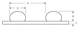
| Package Offering |
| |
 |
| |
| Pitch (mm) |
Ball diameter (mm) |
Ball height (mm) |
Die thick. (mm) |
Ball size (mm) |
| A |
|
B |
C |
D |
| 0.50 |
0.3 |
0.24 |
0.33~0.73 |
0.32 |
| 0.50 |
0.35 |
0.28 |
0.33~0.73 |
0.38 |
| 0.65 |
0.35 |
0.28 |
0.33~0.73 |
0.38 |
| 0.75 |
0.50 |
0.39 |
0.33~0.73 |
0.54 |
| 0.80 |
0.50 |
0.39 |
0.33~0.73 |
0.54 |
|
|
| Material |
| |
| UBM: Al/NiV/Cu |
| Solder ball: Eutectic Pb/Sn, leadfree |
| Flux: Water soluble flux |
|
| Standard Process |
| |
| First dielectric layer coating/exposure/developing |
| UBM sputter deposition |
| Cap photolithography |
| Cap metal etch |
| Second dielectric layer coating/exposure/developing |
| Wafer grinding (Optional) |
| Wafer laser marking (Optional) |
| Wafer ball mounting |
| Wafer sawing (Optional) |
| Final Inspection (Gate) |
| Packing |
|