| Product Overview |
| |
FCCSP (Flip Chip Chip Scale Package) offers chip scale capacity for I/Os around 200 or less. FCCSP provides better protection for chip and better solder joint reliability compared with direct chip attach (DCA) or chip on board (COB). FCCSP is more superior to known good die (KGD) in low-cost test and burn-in, and performs comparable electrical function with KGD. FCCSP features thin and small profile, and lightweight packages.
Applications include RFICs and memory ICs. ASE provides packaging service for any customer-designed size at ball pitches ranging from 0.5 to 1.0mm, and no. of I/Os from 16 to 200. The types of encapsulation are underfi ll and overmold. |

|
| Application |
| |
Consumer
Camcorders
Digital Camera
DVD
WiMAX
Computer
Voltage regulators
High-speed Memory
Card
PC Peripherals
Telecommunication
Pagers
Cellular handsets
GPS |
|
| Features |
| |
| Thinner Profile |
“Wafer Thinning” capability (down to 6~8 mils) to support packages thinner than 1.0 mm |
| Substrate |
2-layer BT laminate substrate is used to reduce overall package cost |
| Improved Performance |
Thin core (100um) substrate & via-on-pad design can be adopted to achieve better electrical performance |
| Robust Structure |
Overmolded process can enhance throughput, component and board level reliability |
| NSMD with OSP C4 pad |
Low cost solutions for electric interconnect between solder bump and substrate |
|
|
| Reliability |
| |
| Package Level |
| MSL Level 3 |
220 °C |
| TCT-B |
1000 cycles |
| THT |
1000 hrs |
| HTST |
1000 hrs |
| PCT |
168 hrs |
| HAST |
100 hrs |
|
| |
| Board Level |
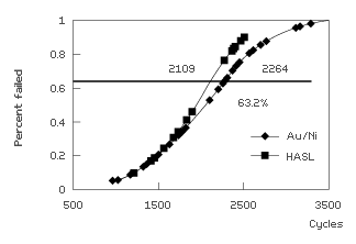 |
• Weibull distribution of FCCSP 48L with different surface fi nish
• 0.30 mm dia. SN63/Pb37 solder ball
• Test Condition: -40 ~ 125 deg. Celsius air-to-air
• Ball composition of LF35 or SAC105 were applied on green /RoHS package |
|