| Cavity-Down Thermally Enhanced BGA |
| |
Cavity-Down Thermally Enhanced BGA is the solution for thermal dissipation requirements of over 6W. It is designed with the chip seated onto the copper heat sink to absorb the heat easily. This method desensitizes the performance deviation out of the chip size and lowers the thermal resistance of junction-to-case (θJC), which makes the external heat sink or fan work more effectively.
ASE's Cavity-Down BGAs are offered through L2BGA and CSBGA. Both open tool and close tool are available. In general, Cavity-Down BGA enhance thermal performance by about 15~20% improvement compare with to 4-layer PBGA and by 35% compare with 2-layer PBGA. Electrical performance of Cavity- Down BGA is significant as well. The reason is attributed to their flexible layout for staggered traces on different layers, shorter VIAS and better shielding effect out of the copper heat sink. With the heat sink covering the signal traces fully, Cavity-Down BGA provides better resistance to external EMI (Electro- Magnetic Interference) noise.
Cavity-Down BGA is an excellent solution for graphic, networking, and communication ICs with high-power and high-speed quality performances. |

|
| Cavity Down BGA Feature |
| |
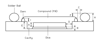 |
| Symbol |
Description |
Criteria |
Remark |
| A |
Die thickness |
15 mils ± 1 mil |
|
| B |
Epoxy thickness |
2~4 mils |
|
| C |
Distance between encapsulation edge
to solder ball |
10 mils (Min.) |
|
| D |
Die edge to cavity |
25 mils (Min.) |
|
| E |
Cavity depth |
25 mils nom |
|
| F |
Clearance between
compound & ball
(Stand off) |
1.27mm ball pitch with 0.75 mm
solder ball
0.1mm (4mils) min. |
|
1.0mm ball pitch with 0.63 mm
solder ball
0.1mm (4mils) min. |
| H |
Solder ball height |
1.27 mm ball pitch |
0.6 ± 0.1 mm
Pad Opening = 0.55 mm |
Solder ball defined
is required. |
| 1.0 mm ball pitch |
0.5 ± 0.1 mm
Pad Opening = 0.40 mm |
| I |
Loop height |
1.27 mm ball pitch with
0.75 mm solder ball
12 mils max. |
In line ≤ 4 wire groups (Ring + Finger)
Staggered ≤ 3 wire groups (Ring + Finger) |
1. All inner pads
must bond to outer finger only. |
1.0 mm ball pitch with
0.65 mm solder ball
10 mils max. |
In line ≤ 3 wire groups (Ring + Finger)
Staggered ≤ 2 wire groups (Ring + Finger) |
2. Solder mask
between rings is
required. |
| G |
Substrate thickness |
L2BGA: 1.1mmCSBGA: 0.97mm |
|
|
* Ball pad  solder mask defined is required. solder mask defined is required. |
| * Finger/Ringsolder mask between rings is required. |
|