 |
|
|
| Substrate Design Services |
 |
Overview
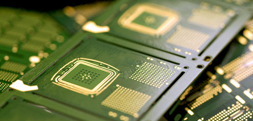
As customers are demanding small, thin, and high performance for their electronic products, device makers are searching for high performance, high reliability, and low cost solutions. Substrate/lead frame has played a very important role in packaging industry, not only because it represents a great portion of the cost, but also because it has a great influence on package performance. How to design a high performance, low cost substrate/lead frame has become one of the major tasks in all packaging companies. In ASE, we have a group of experienced professional dedicate in substrate/lead frame design in order to provide turnkey solutions for our customers to fulfill high performance, cost saving and short time to market.
Function & Service
Failure Mechanism Analysis
- Cu Alloy and lead-free lead frame design: We not only offer services in traditional packages like PDIP, PLCC, QFP, TQPF, SO, but also provide fine pitch (0.16mm), Lead on Chip (LOC), Multi-frame LOC, Exposed Pad L/F, Ground Bunced L/F, Fused, Drop-in Heat Spreader Type L/F, Attached Heat Spreader Type L/F, and Side by Side, Stacked Type MCM Lead Frame.
- Lead less Lead Fame design: Lead less lead frame can be used for packages using QFN (MCP/MCC), BCC/BCC+/BCC++.
- Tape Carrier: Except for the metal lead frame we mentioned above, ASE also provide design service for Tape base material, include Film (Flux), Substrate, Tape BGA, COF, TCP, and uBGA.
- Customize Carrier Design: We provide customize designs for LBGA, TFBGA, CSP, Side by Side, Stacked (or both) MCM substrate. At the same time, we also do all kind of measurement and simulation for customers to fulfill device operation requirement.
- As our many professional and experiences RD members working on carrier design, we also connect with carrier manufactures all over the world to produce the lowest cost, highest performance, and best reliability carriers to our customers.
|
 |
Design Tool
The characteristics of packaging material are a major concern when determining how well the ICs will perform. ASE's Material Laboratory provides the characterization analysis of the following properties. The related instruments are listed next. Users can find more information from the Measurement Equipment section.
- Design information format:
• GDS II
• Microsoft office format netlist
• Pad coordinator
• Ball out
- Design tool:
• Cadence
• Xynetix
- Drawing offering:
• Layout Drawing:
» AutoCad R14
» 2000 Gerber RS 274X
» Acrobat, pdf Format
• Bonding Diagram:
» AutoCad R14, 2000
» Acrobat pdf Format |
|
|